As the name indicates , a sample and
hold circuit is a circuit which samples an input signal and holds onto
its last sampled value until the input is sampled again. Sample and hold
circuits are commonly used in analogue to digital converts,
communication circuits, PWM circuits etc. The circuit shown below is of a
sample and hold circuit based on uA 741 opamp , n-channel E MOSFET
BS170 and few passive components.
Description
As the name indicates , a sample and
hold circuit is a circuit which samples an input signal and holds onto
its last sampled value until the input is sampled again. Sample and hold
circuits are commonly used in analogue to digital converts,
communication circuits, PWM circuits etc. The circuit shown below is of a
sample and hold circuit based on uA 741 opamp , n-channel E MOSFET
BS170 and few passive components.
In the circuit MOSFET BS170 (Q1) works
as a switch while opamp uA741 is wired as a voltage follower. The signal
to be sampled (Vin) is applied to the drain of MOSFET while the sample
and hold control voltage (Vs) is applied to the source of the MOSFET.
The source pin of the MOSFET is connected to the non inverting input of
the opamp through the resistor R3. C1 which is a polyester capacitor
serves as the charge storing device. Resistor R2 serves as the load
resistor while preset R1 is used for adjusting the offset voltage.
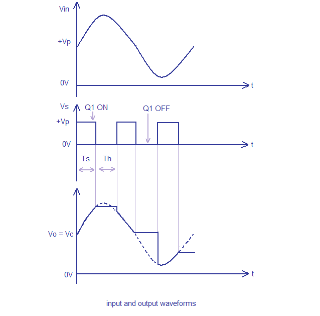
During the positive half cycle of the
Vs, the MOSFET is ON which acts like a closed switch and the capacitor
C1 is charged by the Vin and the same voltage (Vin) appears at the
output of the opamp. When Vs is zero MOSFET is switched off and the only
discharge path for C1 is through the inverting input of the opamp.
Since the input impedance of the opamp is too high the voltage Vin is
retained and it appears at the output of the opamp.
Circuit diagram
Sample and Hold circuit using uA741 opamp
Input and output waveforms.

Input and output waveforms - Sample and hold circuit
Notes
- The circuit can be assembled on a vero board.
- Use +15V/-15V DC dual supply for powering the opamp.
- Capacitor C1 must have minimum leakage current possible and thats why a polyester capacitor is used here.
- Mount the IC uA741 on a holder.
- The type number of the MOSFET Q1 is not very significant here and so substitution is possible if BS170 is not available.
- BS170 is a 60V, 500mA n-channel enhancement mode MOSFET available in TO-92 package.
- Preset resistor R1 can be used for offset adjustments.


0 comments:
Post a Comment